I regret how long this has been taking me, but work has been driving me nuts lately, and I’m also doing my best to teach myself how to design the printed circuit boards I want to incorporate into these props. After a few days of work, I think I have a good solution designed!
The parts I’m trying to combine, condense, or otherwise interface are as follows:
- Teensy 3.2 Microcontroller;
- ILI 9341 TFT display (Without PCB);
- 400 mAh LiPo battery;
- LiPo battery charger based on this design from Sparkfun;
- 8.0 Ohm Speaker;
- 1.4W Class D Amplifier based on this design from Sparkfun;
- Neopixel LED;
- Two red SMD LEDs for the sides of the device rails;
- 3 Buttons – two that trigger effects on the prop, a third for power.
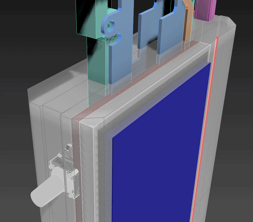
This all has to be crammed into a rather specific area of the prop, which dictated some of my layout of the board. Here’s a look at everything contained within the device – the relevant electronic components are highlighted. I do not have the neopixel or buttons on this 3D model yet, but that isn’t major.
The pink cube next to the Teensy is the 400 mAh LiPo battery. In terms of positioning, everything is pretty much where it needs to be. I know I have some empty space above the components, but I need that space clear, as the whole top half of the device needs to be able to slide in and out with a spring-loaded mechanism.
Here’s a look at the whole board before we dive in:
THE CHARGER
I started with Sparkfun’s Eagle files for their Micro-USB charger. This is built around the MCP73831 chip. Stuff I observed on this: There’s one leg on the chip that is labelled “PROG” which allows you to control the conditioning and charge of the LiPo battery. SparkFun’s default has a 2.0k resistor in that position, which apparently sets the rate at 500mA. A 10k resistor in that spot apparently drops the rate to 100mA. I had some concerns about trying to charge a 400mAh battery like what I’m using with the 500 mA rate, but I’ve had one of these things set up on a breadboard for a few weeks now and it seems to work without any issues, so screw it, the 2k resistor looked fine.
There is another leg on the MCP73831 labelled “STAT” which appears to show the charging status via a small red LED on the board. If I understand it correctly (and I may not) I think voltage flows through the LED as per normal while the device is charging into that leg, which is LOW during the process. The chip sets a logical HIGH on that leg when the LiPo is done charging. I tried to keep this LED on my board, and positioned it right underneath the MicroUSB connector on the Teensy 3.2 board.
Speaking of that, I ditched the MicroUSB connection entirely from the SparkFun Lipo Charger. The Teensy already has a microUSB plug, and you can sever the trace on the bottom of the board between the VUSB input and the VIN on the Teensy. This means if you plug the Teensy’s MicroUSB plug into a power source, you can then route the power through the LiPo charger connections, allowing you to charge the device.
I have breadboarded this and found everything to work OK so far – the wire I’m holding is the one I connect to the Teensy VIN on my breadboard to complete the connection, as I don’t have a slide or toggle switch spare to test things with. Whether the device is on or off, if it’s plugged into the MicroUSB port on the Teensy the battery should be getting charged. The Teensy MicroUSB is oriented pointing downwards, and I’m going to make a cutout in the bottom of the device so you can plug a normal cell phone charger into the thing to top it off. Should work nicely!
I trimmed some parts of the Sparkfun design away – got rid of the JST connector because I intend on simply soldering the LiPo battery wires to the final board. This stuff is all located on a section of the PCB that is in a ‘channel’ between the Teensy and the LiPo battery.
If I moved it farther to the right, the LiPo battery would basically end up being on top of the area I wanted to connect things to, which would have been no good in terms of managing the available space I had. Here’s an image just highlighting the charging circuitry on the board. I think this should work, but I genuinely don’t know. Assuming I have done this right, a switch will be connected to each pad of the “PWRSWITCH” area; when connected, the device should turn on. If not connected, but plugged into the Teensy’s MicroUSB, the device should still charge the LiPo.
THE AMPLIFIER
Lorem ipsum dolor sit amet, consectetur adipiscing elit. Ut elit tellus, luctus nec ullamcorper mattis, pulvinar dapibus aFor this, I started with Sparkfun’s Eagle files for their Mono Amp. It’s built around a TPA2005D1 chip. The chip has audio IN+ and IN- pins, audio OUT+ and OUT- pins, VCC, and GND, which are easy enough and I think I got them sorted. There’s also apparently a pin labeled “NC” for No Connection, and the datasheet says it still needs “a pad and trace”. I don’t get why that’s on there, but I guess it’s more for mechanical attachment purposes than anything. Lastly, there’s a “SHUTDOWN” pin that disables the device – it describes it as “active low logic”. Best I can tell is that while this pin is HIGH, the amp is on – if the pin goes LOW, the amp turns off. When I ground that pin on my Sparkfun Amp on my breadboard, this seems to be the case. I never want the amp to turn off – if the device is on, it should be on – so I got rid of a couple of things from the Sparkfun board. Basically, the way I have it on my own board is that the amp should always be HIGH, and therefore on, assuming I’ve done this right. The Sparkfun design had a decoupling cap as close as possible to the chip on the output side of the chip, so I did the same thing.
This image should highlight the amplifier. I connected the IN- pin to the AGND (analog ground) pin on the Teensy after some experimenting with my breadboard. If I connected it to the universal ground line, I got a lot of noise whenever the screen or other components did something. Hooking the IN- to AGND quieted everything down, as I guess the Teensy isolates that ground through a ferrule on its own board. I did my best to avoid crossing lines or anything other than a ground plane under any of the amplifier stuff to hopefully reduce any kind of EMI or other noise, though I had to make one little concession from the decoupling capacitor by the output over to VCC. The audio input is driven by the DAC pin on the Teensy (can’t be moved, unfortunately), which is a digital-to-analog-conversion pin that can output a nice sine waveform for the speakers, in contrast to the usual digital pins that spit out square waves. Made the audio output a lot cleaner sounding.
As with the power connections, I put soldering pads on the strip of PCB that will be exposed between the Teensy and the LiPo battery. Figured I’d have enough room there without the wires being in anything’s way.
THE TFT BREAKOUT
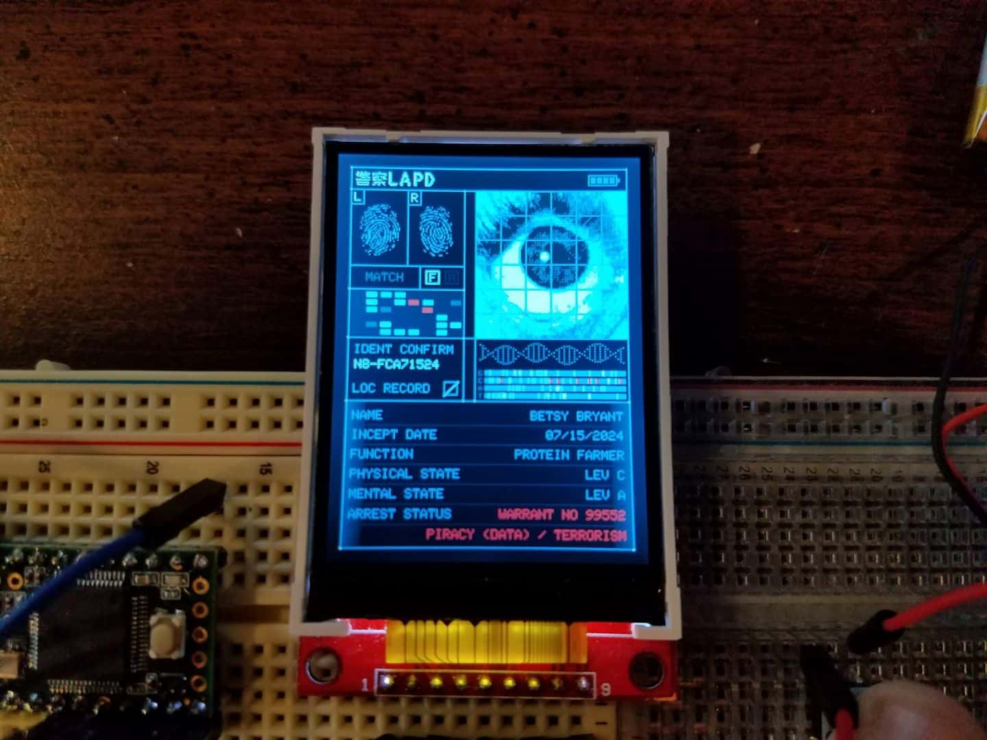
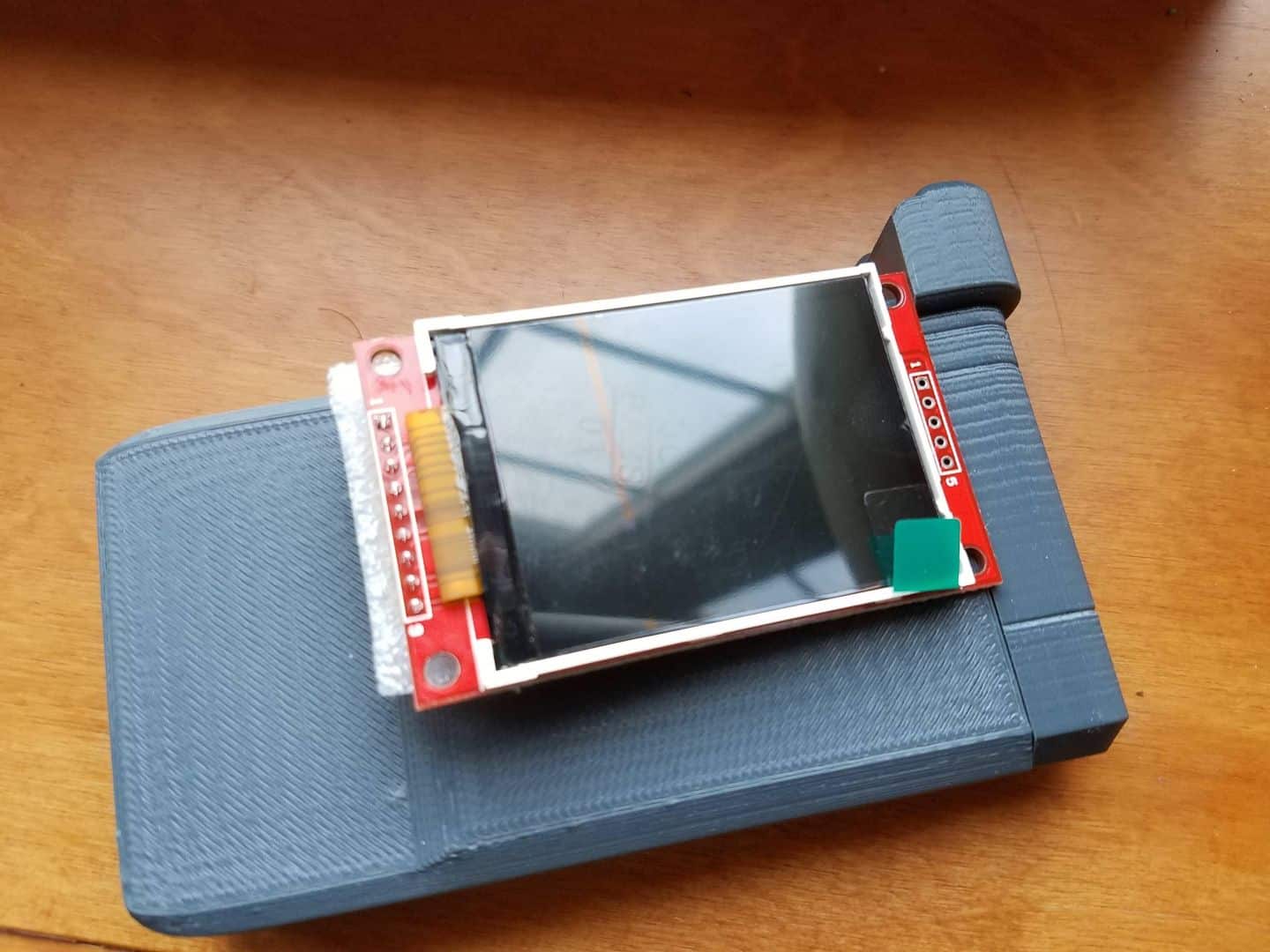
I’m using 2.4″ non-touch ILI9341 boards with those obnoxious ribbon cables. In contrast to the rest of the board, this ribbon cable is going to be attached to the back of the board, to preserve the orientation of things inside the device. I know the usual way of attaching these things to PCBs is to fold the ribbon under the screen and solder it down, then attach the screen with double-sided tape to the PCB. I need that area behind the screen clear for the moving components of that sliding pop-out bit on the device, so that’s not an option. The screen is going to fit snugly into the frame of the device I’m designing for it, and probably get hot-glued in around the edges. I was a bit nervous about the precision aspects of trying to line 18 .8mm pitch pins up with the board, so came up with a bit of a solution.
The solder pads for the ribbon cable were made longer so that if there was a bit of variation in the length of how the ribbon cable hung below the screen I could have a bit of leeway moving things up and down. I also added two oval cutouts on the PCB that I intended on putting some M2 (2mm diameter) screws through; this would let me mount the board inside the device at two fixed spots, but I could move the PCB a few mm to the left or right to make sure the ribbon/pins/pads/display/display bezel all lined up like they should. Basically just tried to leave a bit of room for things to be adjusted if necessary.
In my code for the TFT, I use the following declarations:
#define TFT_DC 9
#define TFT_CS 10
#define TFT_MOSI 11
#define TFT_MISO 12
#define TFT_RST 7
#define TFT_CLK 13 //Arduino SCK
#define TFT_LED 6
The LED control is done on pin 6 through a small 10 ohm resistor. VCC on the Teensy is 3.3V, so I figured that’d be fine, and it looks like the Teensy’s pins can put out the necessary current for the backlight LEDs. It lets me control screen dimming/brightness in-program. All the rest of the pins are pretty much in a good position to run to the board, with the exception of TFT_CLK (the SCK pin), which seems to be pretty specifically keyed to Pin 13 for some reason. I tried moving it around to a different pin, didn’t go well. Not a big deal, just inconvenient.
The last 4 pads for the ribbon cable are for the touchpad stuff, and are basically not hooked up to anything because the displays I’m using don’t have a touchscreen layer built into them. I could ground them, but I wasn’t sure if I should.
AND ALL THE REST
I’m also using these definitions in my code:
#define SCAN_PIN 15
#define PAGE_PIN 14
#define NEO_LED_PIN 5
// 330 Ohm resistor on the data-in pin of the Neopixel works well for Teensy 3.2
I have two buttons – one changes a page on the screen to different information (“PAGE BUTTON”) and the other makes the device ‘scan’ a target ( “SCAN BUTTON”, flashes the neopixel LED, turns the screen white, plays sounds). Those are at the top of the board on the pins “PAGE” and “SCAN”, and hooked to pins 14 and 15 to be consistent with the above declarations. They touch VCC through 10k Ohm resistors to pull them up, and the buttons for each will go from their pins, through the button, and to ground to trigger them. This is part of why I put a bunch of spare GND pins on the top of the board as well.
The Neopixel is a single unit. Needs 3 pins – VCC, GND, and one to carry a data signal. The VCC and GND are built into the top right corner of the board, and the Data pin is next to them, being driven from Pin 5 on the board (to the left of the TFT solder pads). Best practices suggest that you put a 420 ohm resistor in line with the data – I dropped a 330 onto the board because that’s what my breadboard setup uses and it seems to work fine for a single LED. Best practices also suggest a decoupling capacitor between the VCC and GND for the Neopixel (specifically, they suggest a .1uF cap right beneath the neopixel) but I figured the 10uF one on the Amp that’s also connected to the same VCC pin would be enough.
I had a bunch of unused pins on the left side of the board (pins 16-23 on the Teensy). I got rid of them and instead put a row of spare VCC and GND connections in case I needed to hook extra stuff up to the board (ex detail SMD LEDs that turn on when the device is on). These are offset from the pins on the Teensy so I don’t get confused and accidentally put header pins through to connect these.
That’s it in a nutshell. If any of you are electrical engineers and want to double-check this board and save me the headache of ordering them, waiting a few weeks, getting them, and having them not work, I’d appreciate an extra set of eyes. I’m literally teaching myself how to do all of this as I go, and lord knows there’s probably some conventions or rules I’m violating with this design, so someone with more experience is essential. Still, I’ve got a reasonably good hunch this will work?


